
The C74-6502 has been optimized to have a critical path of just 50ns (which translates into a 20MHz maximum clock-rate). The optimization effort was guided by an on-going analysis of the critical path through the CPU for various logic families, as follows:
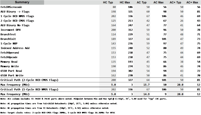
The table above lists the logic paths that signals take through the CPU, and calculates the Total Propagation Delay (tpd) for each. To do so, each IC in the path is considered and it’s associated tpd counted towards the total. Different 7400 logic families operate at varying speeds, so the table is arranged to show the Typical and Max tpd figures associated with HC and AC logic families, as well as one column labelled “AC+” to denote mostly AC logic with a selected LVC and CBT parts. The column labelled “AC+ Typ” reflects the CPU’s final 50ns critical path. (See C74-6502 cycle times for a detailed look at every signal path and its associated propagation delay).
Several important optimizations were required to achieve the 50ns goal, as follows:
- A two-stage Microcode Pipeline is used to eliminate the delay associated with fetching microcode from Control ROMs. ROM access speeds are in the order of 45ns, which is much too slow for a 50ns cycle. To overcome this problem, the C74-6502 pre-fetches microcode one-cycle ahead and overlaps the FETCH and EXECUTE portions of the cycle so they occur concurrently. The pipeline thereby makes sure new microcode is always available at the start of the cycle and the Control Unit can proceed without delay . (See C74-6502 Microcode Pipeline Notes for more details).
- 1-cycle BCD adjust logic (& bus pre-loading) … details to come
- Skip Adder, … details to come
Construction Considerations
- SOIC Packages to keep the assembly small and traces as short as possible
- 4 layer PCB with GND and VCC planes
- Bypass caps on every IC. A 4.7uF capacitor is placed close to the VCC intercard pins on each card.
- Clock signal buffering and load management: each CPU card generates its own buffered local clocks based on the cross-card clock signals. The buffers reduce load on individual clock signals and help minimize skew across the various cards. All use a single gate delays to synchronize clocks across cards. (See C74-6502 Clock Loads)
- Inter-card connectors with generous grounding: signals on these connectors are arranged in a regular pattern (GND, SIG, SIG, GND) such that every signal has either a GND (or a bypassed VCC) pin next to it.
Miscellaneous Improvements
- CBT, LVC Logic Family parts
- Shadow Address Registers to reduce propagation delay to the external address bus (See Card A – Registers)
- Bus Management scheme to avoid transient collisions (see Card A – Registers)
