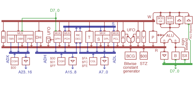
 The C75-6502’s internal bus structure is fairly straight forward — there are two main buses (shown in red above): the W-BUS is used to write to all registers, and the R-BUS to read from them. The ALU takes register values on the R-BUS, together with external values from memory (via the Data Bus D7..0), and outputs its results to the W-BUS, ready to be written back to the registers. The internal address buses (ADL, ADH and ADX shown in blue above) take their input from internal address registers, and output to the external address bus (A0..A23). Finally, the S-BUS (also shown in blue above) receives the output of a 16-bit address incrementer (INC/DEC above) for address handling. The incrementer takes its input from the internal address bus, ADL/ADH.
Main CPU Registers (Card A)
- A, X, Y — User registers
- P, S, T — Status, Stack Pointer and Temporary registers
- PCL, PCH — 16-bit Program Counter
- DPL, DPH — 16-bit Data Pointer
Address Bus Extension (ADX) Registers (Card C)
- DH — Direct Page Register
- PBR, DBR, TBR — Program, Data and Temporary Bank Register
- B — B Accumulator
Other Block Diagram Elements (Card A)
- CGL, CGH, CGH (ADX), STZ, BCG — Constant Generators
- INC/DEC — Dedicated 16-bit address incrementer
Other Block Diagram Elements (Card B)
- DPH+1, A&X — Special registers for Undocumented Opcodes
- SX — Sign Extension buffer for branch address calculation
- SHR, ROR — ALU shift right function
- BCD Cor. — ALU Binary Coded Decimal Correction Logic